Cirrus-logic CS4362 Manuel d'utilisateur
Naviguer en ligne ou télécharger Manuel d'utilisateur pour Matériel Cirrus-logic CS4362. Cirrus Logic CS4362 User Manual Manuel d'utilisatio
- Page / 42
- Table des matières
- MARQUE LIVRES
- Features 1
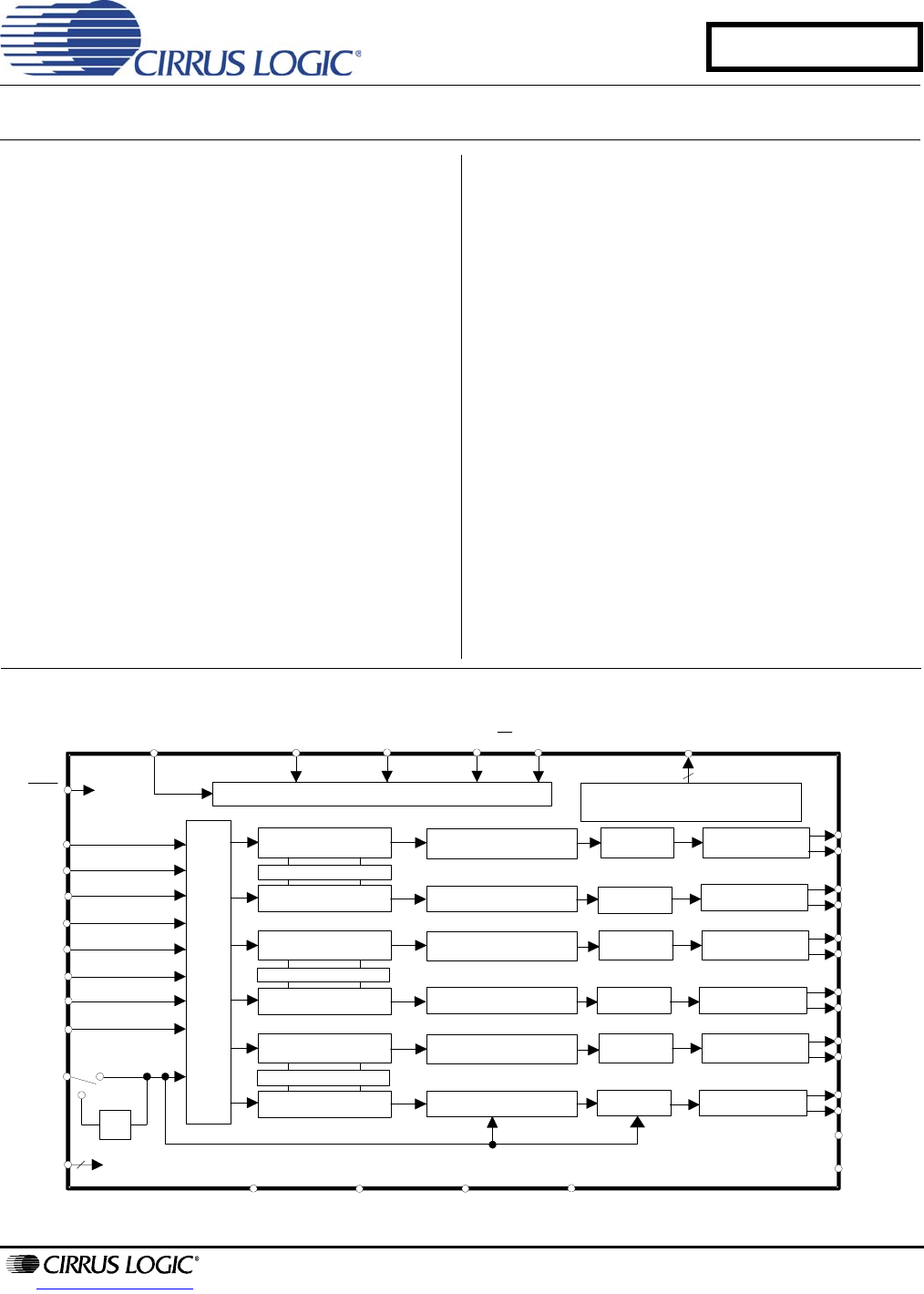
- Description 1
- TABLE OF CONTENTS 2
- LIST OF FIGURES 3
- LIST OF TABLES 4
- ANALOG CHARACTERISTICS 5
- ANALOG FILTER RESPONSE 7
- DIGITAL CHARACTERISTICS 8
- ABSOLUTE MAXIMUM RATINGS 8
- SWITCHING CHARACTERISTICS 9
- DSD_L, DSD_R 10
- Note*: Necessary for I 13
- +3.3 V to +5 V 14
- 3. REGISTER QUICK REFERENCE 15
- 4. REGISTER DESCRIPTION 16
- 4.1.5 Power Down (PDN) 17
- 10000100 18
- 76543210 18
- 4.3.5 Auto-Mute (AMUTE) 20
- 4.6.3 Functional Mode (FM) 23
- 4.7.1 Mute (MUTE) 23
- 4.7.2 Volume Control (xx_VOL) 23
- 24 DS257F2 24
- 1110 - CS4362 24
- Function: 24
- 5. PIN DESCRIPTION 25
- 6. APPLICATIONS 28
- 6.6 Clock Source Selection 29
- 6.7 Using DSD Mode 29
- 7. CONTROL PORT INTERFACE 30
- 7.4 SPI Format 31
- 7.4.1 Writing in SPI 31
- 00000000 32
- Amplitude (dB) 34
- 36
- DS257F2 37 37
- 38 DS257F2 38
- DS257F2 39 39
- 10.PARAMETER DEFINITIONS 40
- 11.REFERENCES 40
- 12.PACKAGE DIMENSIONS 41
- 48L LQFP PACKAGE DRAWING 41
- 13. ORDERING INFORMATION 42
- 14.REVISION HISTORY 42
Résumé du contenu
Copyright © Cirrus Logic, Inc. 2008(All Rights Reserved)http://www.cirrus.com114 dB, 192 kHz 6-Channel D/A ConverterFeatures 24-bit Conversion Up to
10 DS257F2CS4362DSD - SWITCHING CHARACTERISTICS(TA=-10°C to 70°C; Logic 0 = GND; VLS = 1.8 V to 5.5 V; Logic 1 = VLS Volts; CL=30pF) Note: 18. Min is
DS257F2 11CS4362SWITCHING CHARACTERISTICS - CONTROL PORT - I²C® FORMAT(For KQZ TA = -10°C to +70°C; VLC = 1.8 V to 5.5 V; Inputs: Logic 0 = GND, Logic
12 DS257F2CS4362SWITCHING CHARACTERISTICS - CONTROL PORT - SPI™ FORMAT (For KQZ TA = -10°C to +70°C; VLC = 1.8 V to 5.5 V; Inputs: Logic 0 = GND, Logi
DS257F2 13CS43622. TYPICAL CONNECTION DIAGRAM DigitalAudioSourceVLSCS4362MCLKVDAOUTA1+108320.1 µF+1 µF+3.3 V to +5 VSDIN191 µF0.1 µF++2021FILT+CMOUT
14 DS257F2CS4362DigitalAudioSourceVLSCS4362MCLKVDAOUTA1+108320.1 µF+1 µF+3.3 V to +5 VSDIN191 µF0.1 µF++2021FILT+CMOUT76LRCK1SCLK1SDIN3SDIN239400.1 µF
DS257F2 15CS43623. REGISTER QUICK REFERENCEAddrFunction7654321001h Mode Control 1 CPEN FREEZE MCLKDIV Reserved DAC3_DIS DAC2_DIS DAC1_DIS PDNdefault00
16 DS257F2CS43624. REGISTER DESCRIPTIONNote: All registers are read/write in I²C Mode and write-only in SPI, unless otherwise noted.4.1 Mode Control 1
DS257F2 17CS43624.1.5 Power Down (PDN)Default = 10 - Disabled1 - EnabledFunction:The entire device will enter a low-power state when this function is
18 DS257F2CS4362DSD Mode: The relationship between the oversampling ratio of the DSD audio data and the requiredMaster clock to DSD data rate is defin
DS257F2 19CS4362Soft RampSoft Ramp allows level changes, both muting and attenuation, to be implemented by incrementally ramp-ing, in 1/8 dB steps, fr
2 DS257F2CS4362TABLE OF CONTENTS1. CHARACTERISTICS AND SPECIFICATIONS ...
20 DS257F2CS43624.3.5 Auto-Mute (AMUTE)Default = 10 - Disabled1 - EnabledFunction:The Digital-to-Analog converter output will mute following the recep
DS257F2 21CS4362Selects the appropriate digital filter to maintain the standard 15 μs/50 μs digital de-emphasis filter re-sponse at 32, 44.1 or 48 kHz
22 DS257F2CS43624.6.2 ATAPI Channel Mixing and Muting (ATAPI) Default = 01001 - AOUTAx=aL, AOUTBx=bR (Stereo)Function:The CS4362 implements the channe
DS257F2 23CS43624.6.3 Functional Mode (FM)Default = 0000 - Single-Speed Mode (4 to 50 kHz sample rates)01 - Double-Speed Mode (50 to 100 kHz sample ra
24 DS257F2CS43624.8 Chip Revision (address 12h)4.8.1 Part Number ID (PART) [Read Only]1110 - CS4362Function:This read-only register can be used to ide
DS257F2 25CS43625. PIN DESCRIPTIONPin Name # Pin DescriptionVD 4Digital Power (Input) - Positive power supply for the digital section. Refer to the Re
26 DS257F2CS4362 VQ 21Quiescent Voltage (Output) - Filter connection for internal quiescent voltage. VQ must be capacitively coupled to analog
DS257F2 27CS4362 *Note: These modes are only available in Control Port Mode by setting the MCLKDIV bit = 1.Mode (sample-rate range)Sample Rate(kHz)MC
28 DS257F2CS43626. APPLICATIONS6.1 Grounding and Power Supply DecouplingAs with any high resolution converter, the CS4362 requires careful attention t
DS257F2 29CS4362variety of musical tastes and styles. The FILT_SEL bit is used to select which filter is used (see the controlport section for more de
DS257F2 3CS43626.2 PCM Mode Select ...
30 DS257F2CS43627. CONTROL PORT INTERFACEThe control port is used to load all the internal settings. The operation of the control port may be complete
DS257F2 31CS43627.4 SPI Format In SPI format, CS is the CS4362 chip select signal, CCLK is the control port bit clock, CDIN is the input dataline from
32 DS257F2CS43627.5 Memory Address Pointer (MAP)7.5.1 INCR (Auto Map Increment Enable)Default = ‘0’0 - Disabled1 - EnabledNote: When Auto Map Increme
DS257F2 33CS43628. FILTER PLOTS 0.4 0.5 0.6 0.7 0.8 0.91120100806040200Frequency(normalized to Fs)Amplitude (dB)0.4 0.42 0.44 0.46 0.48 0.5 0.
34 DS257F2CS4362 0 0.05 0.1 0.15 0.2 0.25 0.3 0.35 0.4 0.45 0.50.020.0150.010.00500.0050.010.0150.02Frequency(normalized to Fs)Amplitude (dB)0.45
DS257F2 35CS4362 0.2 0.3 0.4 0.5 0.6 0.7 0.8 0.91120100806040200Frequency(normalized to Fs)Amplitude (dB)0.2 0.3 0.4 0.5 0.6 0.7 0.812010080604020
36 DS257F2CS4362 0.45 0.46 0.47 0.48 0.49 0.5 0.51 0.52 0.53 0.54 0.55109876543210Frequency(normalized to Fs)Amplitude (dB)0 0.05 0.1 0.15 0.2
DS257F2 37CS43629. DIAGRAMS LRCKSCLKLeft ChannelRight ChannelSDINx +3 +2 +1+5 +4-1 -2 -3 -4 -5+3 +2 +1+5 +4-1-2 -3 -4MSB LSB MSB
38 DS257F2CS4362LRCKSCLKLeft ChannelRight ChannelSDINx654321098715 14 13 12 11 1010654321098715 14 13 12 11 1017 16 17 1632 clocks19 18 19 18Figure 37
DS257F2 39CS4362 SDINxChannelPair xControlDACDACAOUTAx+AOUTAx-AOUTBx+AOUTBx-LRFigure 40. Channel Pair Routing Diagram (x = Channel Pair 1, 2, or 3)ΣΣ
4 DS257F2CS4362Figure 27. Quad-Speed (fast) Transition Band ...
40 DS257F2CS436210.PARAMETER DEFINITIONSTotal Harmonic Distortion + Noise (THD+N)The ratio of the rms value of the signal to the rms sum of all other
DS257F2 41CS436212.PACKAGE DIMENSIONSINCHES MILLIMETERSDIM MIN NOM MAX MIN NOM MAXA --- 0.055 0.063 --- 1.40 1.60A1 0.002 0.004 0.006 0.05 0.10 0.15B
42 DS257F2CS436213. ORDERING INFORMATION14.REVISION HISTORY Product Description Package Pb-Free Grade Temp Range Container Order #CS4362114 dB, 192 kH
DS257F2 5CS43621. CHARACTERISTICS AND SPECIFICATIONSANALOG CHARACTERISTICS(Full-Scale Output Sine Wave, 997 Hz; Measurement Bandwidth 10 Hz to 20 kHz,
6 DS257F2CS4362ANALOG CHARACTERISTICS(Continued) POWER AND THERMAL CHARACTERISTICS Notes:4. VFS is tested under load RL and includes attenuation due t
DS257F2 7CS4362ANALOG FILTER RESPONSE Notes:10. Slow Roll-Off interpolation filter is only available in Control Port Mode.11. Filter response is n
8 DS257F2CS4362DIGITAL CHARACTERISTICS(For KQZ TA = -10°C to +70°C; VLC = VLS = 1.8V to 5.5V)ABSOLUTE MAXIMUM RATINGS(GND = 0 V; all voltages with res
DS257F2 9CS4362SWITCHING CHARACTERISTICS(For KQZ TA = -10°C to +70°C; VLS = 1.8 V to 5.5 V; Inputs: Logic 0 = GND, Logic 1 = VLS, CL = 30 pF) Notes:15
Produits connexes et manuels pour Matériel Cirrus-logic CS4362
 (6 pages)
© 2020, manymanuals.fr. Tous droits réservés | 1.189 s |
 Manymanuals.com
 Manymanuals.de
 Manymanuals.fr
 Manymanuals.it
 Manymanuals.pl
 Manymanuals.cz
 Manymanuals.es
 Manymanuals-pt.com
Commentaires sur ces manuels